COMPANY

- 2008
- March 24, 2008 ISO 9001 certification was acquired
- 2007
- “Middle Pulse Solar Simulator Completed .Developed large area, multi junction type, concentrating type solar with joint development with the National Institute of Advanced Industrial Science and Technology
- 2006
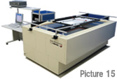
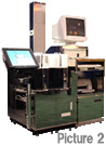
- Started joint development with the National Institute of Advanced Industrial Science and Technology of “Middle Pulse Solar Simulator” for performance inspection for solar cell production line * Picture 15
- 2005
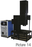
- “Highly approximate type solar simulator” capable of irradiating highly approximate light * Picture 14
- 2004
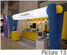
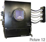
- Delivered a long pulse solar simulator for module calibration to the National Institute of Advanced Industrial Science and Technology * Picture 12 * Semicons booth in 2004 * Picture 13
- 2002
- Delivering solar simulator to NPC Co., Ltd. as a cell tester Held 30 th anniversary party in 2001 Established
- 2001
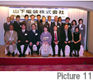
- Holding 30th anniversary party of foundation * Picture 11
- 1996
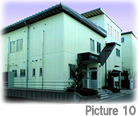
- Miyama factory was expanded, sales and design division moved to Miyama factory * Picture 10 Holding 25th anniversary commemoration party We delivered a large solar simulator to Kitami Institute of Technology in Hokkaido in 1994Holding 25th anniversary party of foundation
- 1994
- Delivered a large solar simulator to Kitami Institute of Technology in Hokkaido
- 1993
- Capital increased to 10 million yen
- 1991
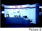
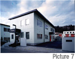
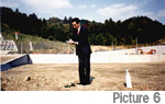
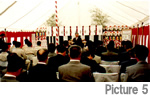
- Capital increased to 10 million yen Heisei 1990 Acquired the land within the Miyama Industrial Park of Miyama Town, moved the manufacturing department holding the 20th anniversary commemoration partyStarted exhibiting at exhibition “SEMICON JAPAN” * Picture 5,6,7,8
- 1988
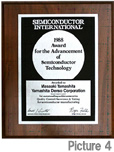
- Establishment of HOLOGENIX in the State of California, USA as a sales base for semiconductor wafer surface defect devices USA Semiconductor surface surface defect device is recognized as “landmark inspection device” in the United States, commended from Semiconductor International * Picture 4
- 1986
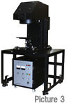
- Capital increased to 8 million yen Started development of solar cell research light source “Solar simulator” * Picture 3
- 1984
- Acquired land in Hachioji City Otsuka, started mass production of relocation “ultraviolet irradiation device” (OEM supply began to be supplied to several major manufacturers) * Picture 1 Started development of “magic” for surface defect inspection apparatus for semiconductor wafers. * Picture 2
- 1977
- Moved to the factory in Hino City, along with the improvement of the manufacturing technology of the lighting power supply, acquired overseas optical technology and began working on manufacturing light sources
- 1974
- Corporate registration with a capital of 2.5 million
- 1973
- Started OEM supply of lighting power supply of special discharge tube to Hachioji analysis equipment manufacturer
- 1972
- We undertook the manufacture of the lighting power supply of the special lamp imported by the foundation trading company in Hino City, Tokyo