
Surface defect inspection system
Surface defect inspection system (normal type)
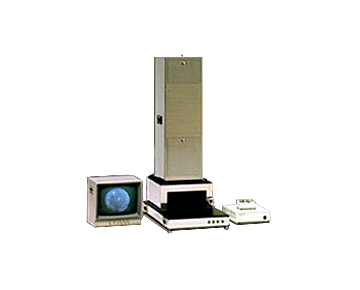
It is a system that can inspect the surface condition of specular planar substrate instantaneously with ultra-high sensitivity, applying the principle of a magic mirror transmitted from long ago, and is used by silicon wafer manufacturers all over the world. The inspection can be done non-contact / nondestructively, and the optical system is maintenance free. Optionally, automatic judgment of surface defects It is possible to add functions such as image processing / automatic conveying mechanism / image storage / image printing.

 It instantaneously expresses all the surface condition.
 Optical system corresponds to Class 1.
 The optical system is maintenance free.
 Detection sensitivity change is possible depending on inspection contents.
| Inspection size | φ 100 mm to φ 300 mm from each model |
| Inspection content Flatness, | dimple, mound, saw mark, orange peel etc. |
| Inspection magnification | 1-3 times mode switching (Standard feature) |
| Detection sensitivity | Continuous detection sensitivity variable |
| Used light source | 550 nm (constant illuminance stabilized light source) |
| Camera | high resolution CCD camera |
| Stage | manual stage (standard specification) |
Utility
| Surface inspection of specular wafer |
| Inspection of slip line |
| Inspection of glass substrate |
| Inspection of other specular substrates |
Option
| Motor driven test stage |
| Automatic defect determination image processing device |
| Image printer |
| Transport mechanism |
- * Demonstration is always available at our company.
- * Sending the sample, it is also possible to return the inspection result by image copy.